- 您现在的位置:买卖IC网 > Sheet目录249 > RT1236B7 (CTS Resistor Products)RES ARRAY 100 OHM 32 RES 64-BGA
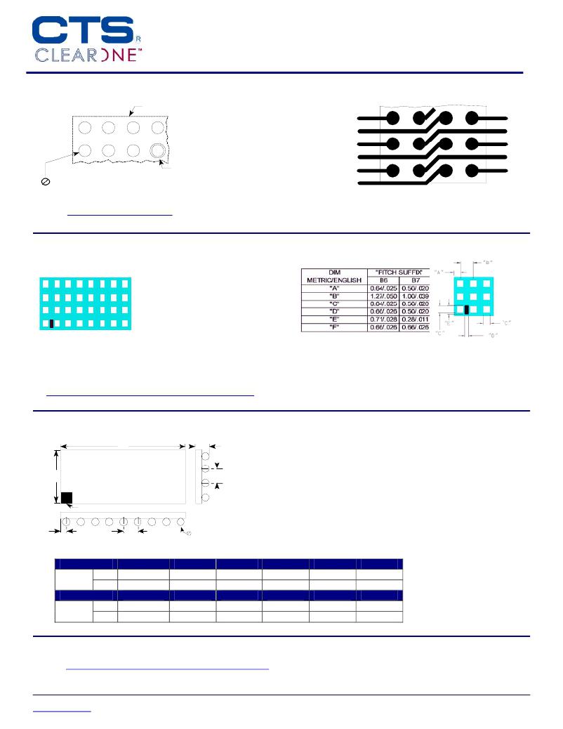
Recommended Land Pattern
BGA Routing Scheme
Outline of Substrate
.005 Inch
Wide Traces
PCB Pad Diameter
Solder Mask Dia = Pad
Diameter +.15mm(.006 inch)
1.00mm Pitch (B7) = 0.51mm/.020 inch (minimum)
1.27mm pitch (B6) = 0.64mm/.025 inch (minimum)
For .006" Thick Solder Paste Stencil, Aperture Opening Should
be Equal to the PCB Pad Diameter.
Refer to www.ctscorp.com/components/clearone.asp for
additional PCB design information
Top Side Probe-able Information
Top Side Probe-able Probe
Pad 4x8 Array Shown
Refer to Top Probe-able
Application Notes for additional
information.
Note: Add a ‘P’ suffix to order Top Side Probe-able version.
Example: RT2203B7PTR7.
Refer to the following link for detailed Top Side Probe-able Information:
www.ctscorp.com/components/clearone/TopProveClearOne.pdf
Mechanical Diagram
L
H
W
RT_2__B7
CTS YRWK
A1 Identifier
P (Pitch)
K
P (Pitch)
D
16 Bit
L
W
H
P
D
K
Style C
32 Bit
Style C
mm
inch
mm
inch
8.00 ± 0.15
.315 ± .006
L
16.00 ± 0.15
.630 ± .006
4.00 ± 0.15
.157 ± .006
W
4.00 ± 0.15
.157 ± .006
1.19 ± 0.15
.047 ± .006
H
1.19 ± 0.15
.047 ± .006
1.00 ± 0.25
.039 ± .010
P
1.00 ± 0.25
.039 ± .010
0.64 ± 0.05
.025 ± .002
D
0.64 ± 0.05
.025 ± .002
0.50 ± 0.25
.020 ± .010
K
0.50 ± 0.25
.020 ± .010
Complete ClearONE Product, Processing, and Application Information can be found at the following link:
http://www.ctscorp.com/components/clearone.asp
? 2006 CTS Corporation. All rights reserved. Information subject to change.
CTS Electronic Components
www.ctscorp.com
Page 2
Memory & IDE Terminator
March 06
发布紧急采购,3分钟左右您将得到回复。
相关PDF资料
RT1250B7TR7
RES NET MULT OHM 16 RES 24-TBGA
RT1300B6PTR7
RES NET MULT OHM 27 RES 36-LBGA
RT1405B7PTR7
RES ARRAY 22 OHM 18 RES 36-TBGA
RT1418B7TR7
RES ARRAY 8.2K OHM 16 RES 24TBGA
RT1452B6TR7
RES NET 25 OHM 32 RES 36-LBGA
RT1710B6PTR7
RES NET 100 OHM 16 RES 32-LBGA
RZB06DHAS
CONN EDGE DUAL .050 R/A 12 POS
RZB120DHFR
CONN EDGE DUAL .050 SMD 240 POS
相关代理商/技术参数
RT1236B7TR13
制造商:CTS Corporation 功能描述:RESISTOR RT1236B7TR13 - Tape and Reel
RT1236B7TR7
功能描述:电阻器网络与阵列 4 X 16 Array RoHS:否 制造商:Vishay/Thin Film 产品类型:Networks 电路类型:Divider 电阻器数量: 电阻数值:10 kOhms 容差:0.1 % 温度系数: 管脚数量:3 工作温度范围:- 55 C to + 155 C 尺寸:1.02 mm W x 3.05 mm L x 1.4 mm H 引线间隔: 端接类型:SMD/SMT 封装:Reel
RT124
制造商:ADAM-TECH 制造商全称:Adam Technologies, Inc. 功能描述:RELAY LOW PROFILE SMT SIGNAL RELAY-TYPE RT1
RT124005F
制造商:MACOM 制造商全称:Tyco Electronics 功能描述:16 Amp PC Board Miniature Relay
RT124006F
制造商:MACOM 制造商全称:Tyco Electronics 功能描述:16 Amp PC Board Miniature Relay
RT124009F
制造商:MACOM 制造商全称:Tyco Electronics 功能描述:16 Amp PC Board Miniature Relay
RT124012F
制造商:MACOM 制造商全称:Tyco Electronics 功能描述:16 Amp PC Board Miniature Relay
RT124018F
制造商:MACOM 制造商全称:Tyco Electronics 功能描述:16 Amp PC Board Miniature Relay
